【封裝基板要做更大,卡在一塊日本玻璃布 🔬】
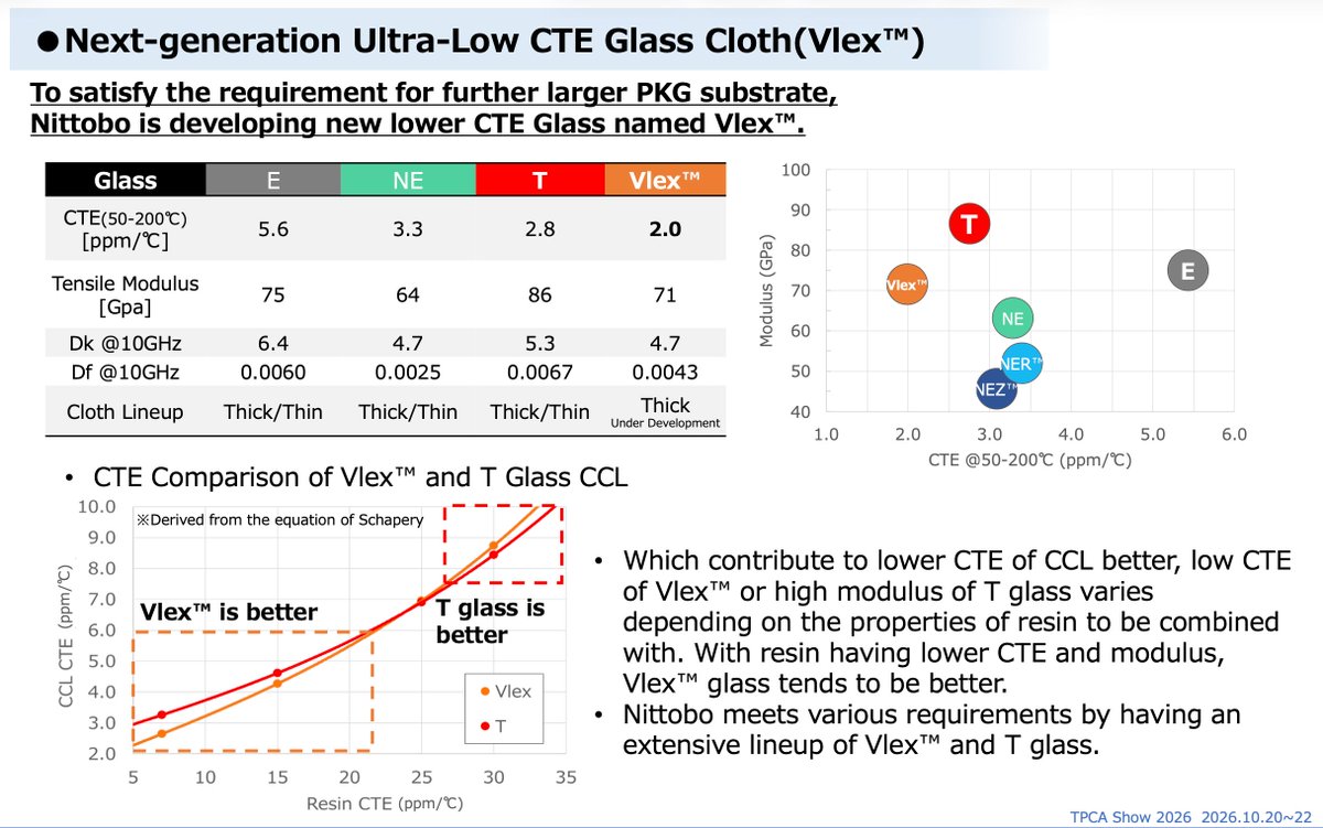
日本日東紡在十月的電路板展上公開了下一代玻璃布 Vlex 的規格:熱膨脹係數 2.0,低於目前高階封裝使用的 T 玻璃 2.8,更低於一般 E 玻璃的 5.6。
封裝基板就是晶片底下那塊板子,由樹脂和玻璃布壓合而成。晶片在製程與運作中反覆加熱冷卻,矽的膨脹係數大約 3,板子如果和它差太多,基板做得越大就翹得越厲害,焊點直接裂開。所以把玻璃布的膨脹係數壓低,等於替基板尺寸解開一道限制,而尺寸正是這一代加速器封裝在搶的東西。
它不是純粹的升級。Vlex 的拉伸模數只有 71,低於 T 玻璃的 86,也就是剛性變差了。日東紡自己在同一頁寫得很清楚:哪一種比較好要看搭配的樹脂,樹脂膨脹係數低的時候 Vlex 占優,高的時候 T 玻璃占優。目前 Vlex 只有厚布,而且仍在開發階段。
人工智慧伺服器的瓶頸清單上,這類材料的名字往往比產能數字更早出現,也更難被取代。
資料來源:日東紡電路板展技術簡報(圖片來自 @SemiAnalysis_)
Bigger Chip Packages Run Into a Piece of Japanese Glass Cloth
At an October circuit-board show, Japan's Nittobo published specifications for its next-generation glass cloth, Vlex: a coefficient of thermal expansion of 2.0, below the 2.8 of the T-glass used in high-end packaging today and far below ordinary E-glass at 5.6.
A package substrate is the board under the chip, pressed together from resin and glass cloth. Silicon expands at roughly 3, and the assembly heats and cools repeatedly. If the board moves at a different rate, a larger substrate warps more and the joints crack. Lowering the cloth's expansion lifts a constraint on substrate size, and size is exactly what this generation of accelerator packaging is fighting for.
It is not a straight upgrade. Vlex has a tensile modulus of 71 against T-glass at 86, so it is less stiff. Nittobo says on the same slide that which one wins depends on the resin: Vlex is better with low-expansion resins, T-glass with the rest. Vlex currently exists only as thick cloth and remains under development.
On the list of bottlenecks for AI servers, materials like this appear earlier than capacity numbers, and they are harder to replace.
Source: Nittobo technical presentation at a circuit-board show (Image: @SemiAnalysis_)